A Groundbreaking First: China's New Advance in the Semiconductor Field
Want to read in a language you're more familiar with?
Lithography is a core driver behind the continuous miniaturization of integrated circuit chip manufacturing processes. Recently, a team led by Professor Hailin...
Lithography is a core driver behind the continuous miniaturization of integrated circuit chip manufacturing processes.
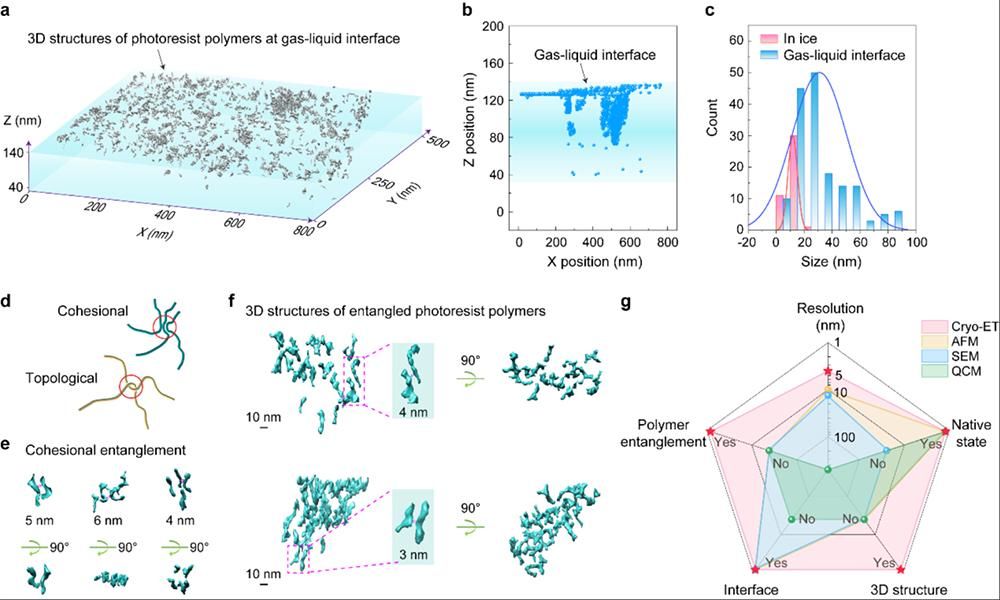
Recently, a team led by Professor Hailin Peng from the College of Chemistry and Molecular Engineering at Peking University, in collaboration with other researchers, has achieved a significant breakthrough. For the first time, they used cryo-electron tomography (cryo-ET) to resolve the microscopic 3D structure, interface distribution, and entanglement behavior of photoresist molecules in their native liquid state. This pivotal discovery has guided the development of an industrial solution that significantly reduces lithography defects. The related findings were published in Nature Communications.
"Development," a crucial step in lithography, involves using a developer to dissolve the exposed areas of the photoresist, precisely transferring the circuit pattern onto the silicon wafer. The movement of photoresist in the developer directly determines the accuracy and quality of this "circuit drawing," ultimately impacting chip yield. Historically, the microscopic behavior of photoresist during development has been a "black box," forcing the industry to rely on repetitive trial-and-error for process optimization—a major bottleneck for improving yields at the 7nm node and beyond.
To address this, the team pioneered the application of cryo-ET in semiconductor research. After standard lithography exposure on a wafer, they rapidly extracted a sample of the developer containing photoresist polymers onto an EM grid. This sample was then vitrified within milliseconds, "freezing" the photoresist in its true liquid state.
Subsequently, researchers tilted the frozen sample inside the cryo-electron microscope, collecting a series of 2D projection images from different angles. Using computational 3D reconstruction algorithms, they merged these images into a high-resolution 3D visualization with a resolution better than 5 nanometers. This method simultaneously overcomes the three major limitations of traditional techniques: the inability to perform in-situ, three-dimensional, high-resolution observation.
This technique led to several critical discoveries. As corresponding author Professor Yiqin Gao explained, while it was previously assumed that dissolved photoresist polymers were dispersed within the liquid bulk, the 3D images revealed they primarily adsorb at the air-liquid interface. The team also directly observed "cohesive entanglement" of these polymers, held together by weak forces or hydrophobic interactions. Furthermore, polymers at this interface were more prone to entanglement, forming aggregated clusters averaging about 30nm in size. These clusters are potential defect sources, as they can deposit onto intricate circuit patterns, causing unintended connections.
The team proposed two practical solutions to control entanglement: optimally increasing the post-exposure bake temperature to suppress polymer entanglement and reduce large aggregates, and optimizing the development process to maintain a continuous liquid film on the wafer surface, helping to wash away polymers and prevent deposition. Combining these strategies successfully eliminated pattern defects caused by photoresist residue on 12-inch wafers, reducing defect counts by over 99%.
Professor Peng highlighted that cryo-ET provides a powerful tool for resolving various liquid-phase interfacial reactions at the atomic/molecular scale. A deeper understanding of polymer structure and behavior in liquids can advance defect control and yield improvement in critical processes like lithography, etching, and wet cleaning for advanced manufacturing nodes.